
2023-09-29
TL;DR: I built a metal detector circuit using only analog components. The circuit that I built works mostly as designed but doesn’t seem to be practical for use in the field. Along the way, I learned a lot about transistors and analog circuit analysis, and I also learned how to make simple printed circuit boards at home. I failed to actually build a practical device—which is frustrating—but I definitely succeeded in my main goal of forcing myself to learn new things.
An LC oscillator consists of an inductor and capacitor in parallel. If the capacitor begins with some charge, then that charge will tend to flow through the inductor. However, the inductor resists this change in current and builds a magnetic field. The magnetic field then collapses, inducing a current in the inductor and charging the capacitor. In this way, the capacitor and inductor trade their energy between the electric and magnetic fields. This oscillation will continue forever if loss is not considered.

The frequency of the oscillation is determined by the magnitudes of the inductance and capacitance in the circuit. This frequency is also called the resonant frequency of the circuit and is given by
where the factor converts the result into hertz, rather than the more fundamental but less familiar unit of radians per second.
A good way to make an inductor is to wrap many coils of wire together. This forces the magnetic field created by the moving electrons to concentrate near the coil. The magnitude of the inductance partly depends on the size of the coil and the number of turns. It also depends on the magnetic permeability of the material nearby. The permeability of air is almost the same as the permeability of a perfect vacuum, so when a wire coil is surrounded by air, not much happens. However, a good portion of typical metals have much higher permeability. When the coil is near one of these materials, the average permeability of the volume near it increases. This makes the inductance increase as well, and the resonant frequency goes down.1
It doesn’t go down by very much, though. Even if the bit of metal has a permeability that’s 500 times higher than air, it still only takes up a small portion of the total volume in the vicinity of the coil. Also, the frequency goes as the inverse square root of the inductance, so the inductance needs to change a lot in order for the frequency to change only a little. In practice, it seems like the maximum change in frequency for a large piece of metal is not more than 2%. We need an accurate way to measure the frequency within that range.
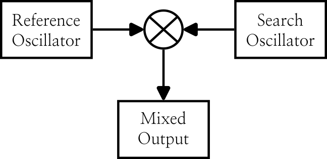
One way to accomplish this would be to use a microcontroller. I didn’t take that approach this time because I wanted to learn more about analog electronics. Instead, I built a beat frequency oscillator (BFO) circuit using three transistors and a few passive components. A beat frequency is the difference between two higher frequencies that are close together. As the high-frequency signals go along, they are sometimes in phase and sometimes out of phase. When they’re in phase, they interfere constructively, and when they’re out of phase, they interfere destructively. This has the effect of creating an amplitude envelope with a frequency equal to the difference between the two inputs.

This property is useful because we can use it to examine the frequency of our search coil by combining it with a fixed reference. If we maintain another oscillator with a frequency that doesn’t change but is near the search oscillator’s frequency, then we can mix them and monitor the beat frequency as a proxy for the search coil. With some forethought, the beat frequency can be designed in the audible range, so the user of the detector can simply listen to the output and interpret it directly. Anecdotally, I seem to be able to detect about a 20 Hz pitch difference under ideal conditions, so maybe in the field it’s more like 100 Hz. That’s much better precision than we can get by examining the search oscillator directly.
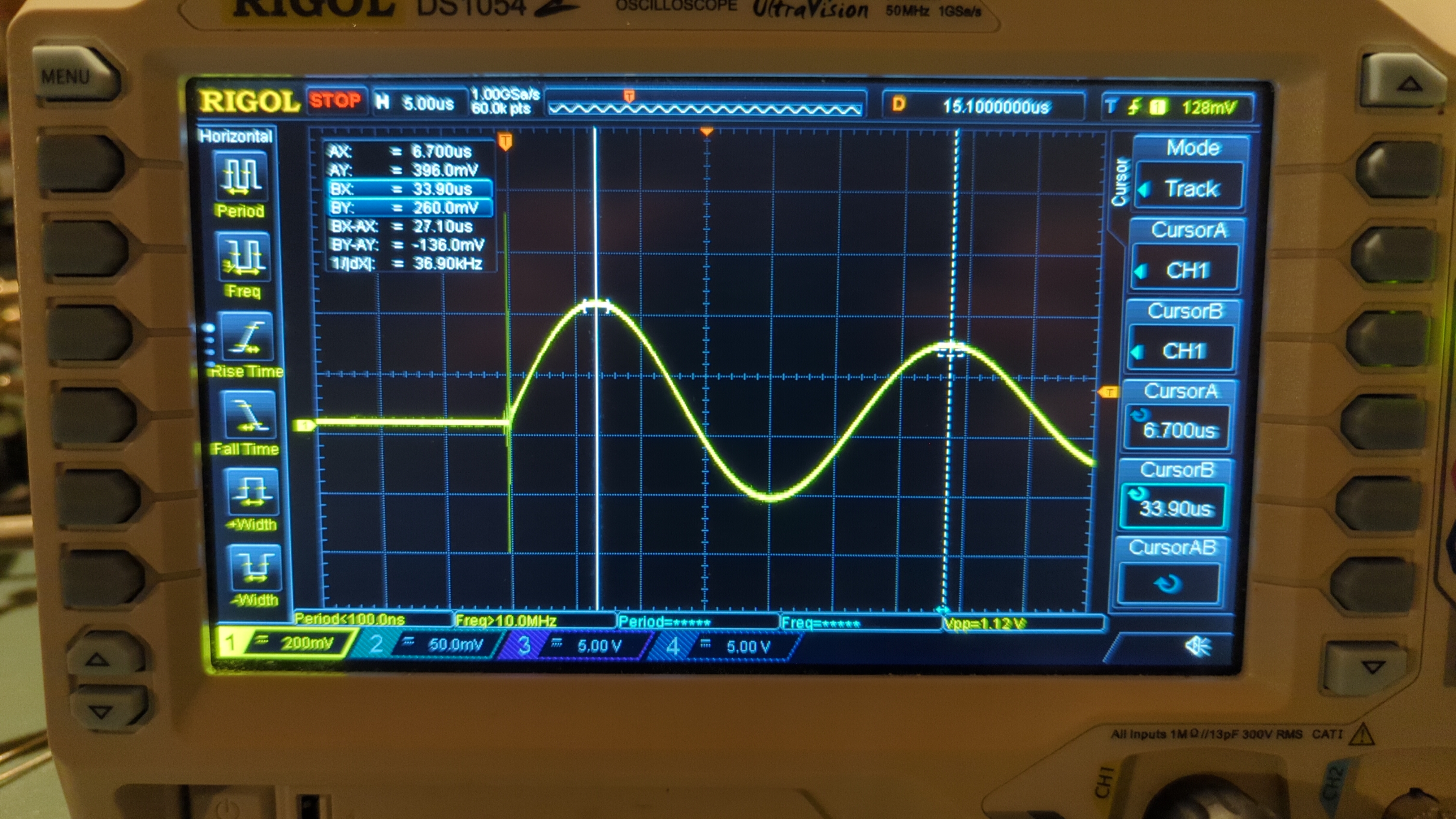
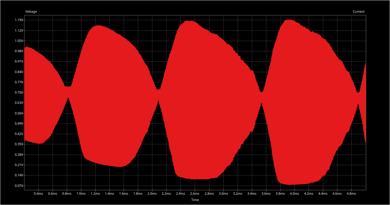
In order to estimate the frequency of oscillation, I need to know the inductance and capacitance of the components in the tank circuit. My multimeter can measure capacitance, but it can’t measure inductance. Fortunately, there’s an easy way to measure an unknown inductance with an oscilloscope and some common circuit elements. I learned this method from this video and modified it slightly.
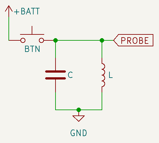
Consider the above circuit. We already know that an LC oscillator has some resonant frequency . By pressing the button and then releasing it, we charge the capacitor and then allow the oscillation to proceed for a few periods. The oscillation will dissipate quickly due to resistive losses and the small component values. With my oscilloscope in single mode, I found that I was able to capture two or three periods of the oscillation. This allowed me to measure . Since is known, I could compute the unknown value of with decent precision.
I think this is analogous to a pendulum. If you move the pendulum away from its resting position and let it go, it will swing with some characteristic frequency determined by its length and the acceleration due to gravity. Eventually, the oscillation will dissipate, but in the meantime you can measure the frequency of oscillation and compute an unknown parameter given the other one.
Using this technique, I was able to measure the inductance of my search coil and modify it as needed to get the value I wanted. I was also able to measure the fixed inductors that I used for the reference oscillator. In general it seems like it’s a good idea to measure the values of critical components because their tolerances are not good, at least for the cheap ones that I had on hand.
The ciruit has three major components:
I used a Colpitts oscillator for this project. The Colpitts oscillator consists of an LC tank circuit and an active element, which keeps the oscillation going. Without an active element, such as a bipolar junction transistor (BJT), the oscillation dies away quickly. The Colpitts design redirects a small amount of the energy in the tank circuit into the transistor, which the transistor amplifies and feeds back into the oscillator. The circuit also ensures that the transistor’s output is in phase with the existing oscillation. These properties satisfy the Barkhausen criteria, which is essential for oscillation.
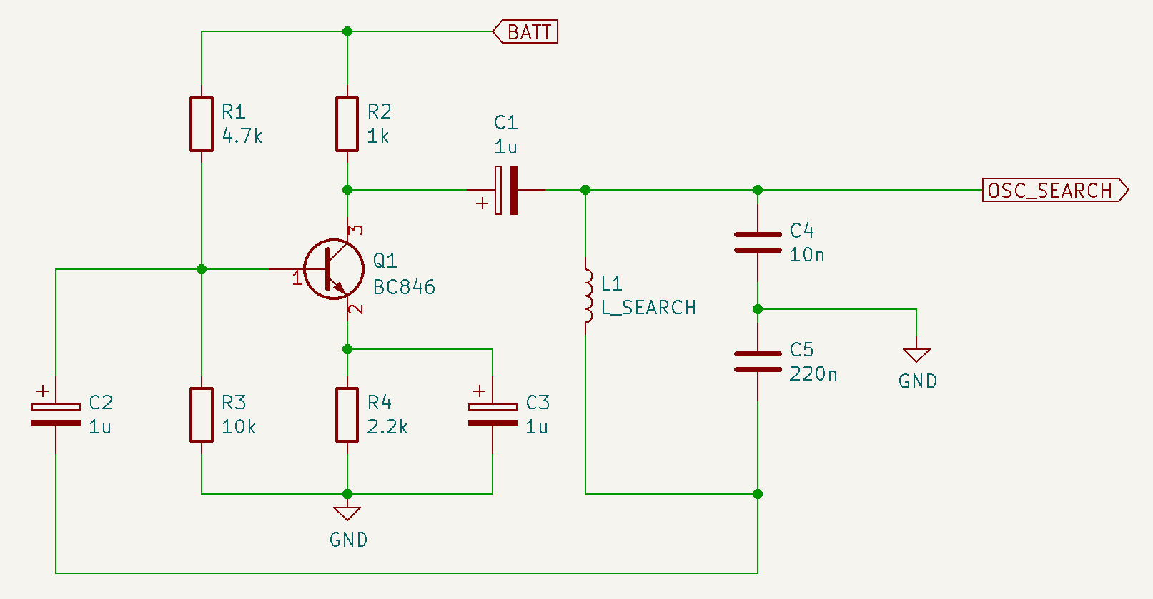
As before, the frequency of oscillation is determined by the choices of and . For this project, the inductor in the reference oscillator is a fixed component, while the inductor in the variable oscillator is the search coil. The two inductance values should be close together in order for the mixed signal to fall in the audible range. I aimed for a frequency of oscillation in the Low-Frequency Experimental Radio band, which is unlicensed in the United States and falls between 160 and 190 kHz. The power radiated by this circuit is probably very low, but I figured I might as well try to resonate at a frequency that’s out of the way.
Mixing the two signals seemed like it would be trivial because electric potential obeys superposition. I thought that this meant that connecting the outputs of the two oscillators together would be good enough, but that doesn’t seem to be the case. Simply summing the high-frequency signals doesn’t actually give a signal that can meaningfully drive a speaker. It’s true that the envelope frequency will be the difference between the frequencies of the inputs, but this envelope is symmetric about the horizontal axis. I assumed that this wouldn’t produce any sound because the speaker element would stay more or less stationary. (Note that I didn’t actually try this, so I could be wrong.) In order for the speaker to produce sound, there needs to be an asymmetry in the signal in the audible range.

There are probably many ways to do this, but I chose one that immediately applied what I had learned about transistor biasing from the Colpitts oscillator. Since the BJT can be used as an element with nonlinear response, we can use it to “cut off” the bottom half of the summed signal, clamping it to zero. I did this by choosing the bias point such that the positive parts of the mixed signal would drive the transistor, while the negative parts wouldn’t. The result is a signal with the desired asymmetry. The average value isn’t zero anymore, and we’ve thrown away half of the usable travel of the speaker element, but we get the tone we want. I think this design is called “unbalanced” and is somewhat similar to a rectifier (although definitely not the same thing)2. I don’t know if this is actually a good design, but it’s kind of neat, and I like that it uses the same components as the rest of the circuit.
I also considered adding a filter to remove the high-frequency components from the output, but then I realized that the speaker is already a low-pass filter. A typical speaker is design to respond in the audible range, so due to the speaker element’s inertia, high-frequency components are automatically smoothed over. Plus, the human ear isn’t sensitive to those frequencies anyway.
A discrete audio amplifier also isn’t necessary here because the BJT can drive enough power to the headphones (a few milliwatts) to be comfortably audible.
I initially built the circuit in Circuit Lab, an online circuit editor and simulator. I normally like to use KiCad, but I had trouble with the simulator. Later, I upgraded my version of KiCad and found it to be much more reliable, so I switched back. One important detail of the simulation is that the voltage source needs to have some noise in order for oscillation to begin. With perfect sources and ideal components, I found that the circuit would get stuck in a metastable state that can’t actually exist in reality. By adding some noise or a small impulse to the voltage source, I was able to nudge the system out of metastability and into more realistic behavior. Once the simulation was producing reasonable results, I had some confidence that my design would actually work.
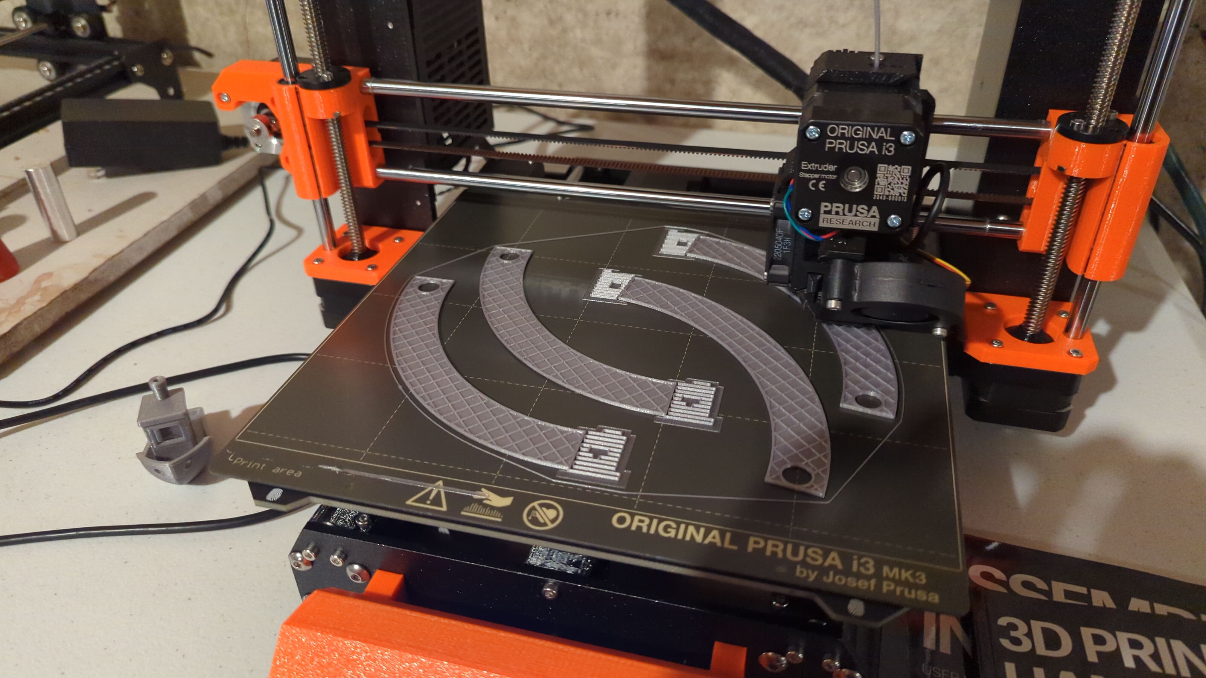
This part wasn’t a problem. I estimated the diameter of the coil (about 9 inches) and CAD’d up a solid of revolution in four identical parts. The resulting hoop had a groove around the outside to encourage the wire to stay put. I designed the hoop sections to be bolted together, and I assumed I’d eventually need to go buy nuts and bolts for that purpose. It turns out that my printer can make those items as well. I downloaded models for an M10 bolt and nut from McMaster-Carr and printed them both. Note that I reduced the size of the bolt to 95% or so of its original size in two of the three dimensions (that is, the non-longitudinal axes) to help with printer tolerances.

After printing, I wrapped on about ten turns of magnet wire and used my inductance measurement circuit to make sure I was close to the target value.
With some confidence that my design would work, I moved on to assembling it on a breadboard. I managed to fit the whole thing on a single large breadboard without too much trouble. I took some extra time to lay the components out logically and cut jumper wires to the correct lengths. This probably took twice as long as it could have, but it was kind of nice to put so much effort into making this iteration look attractive. I didn’t have to think that hard, so I was mostly just working with my hands on a task that required some precision. When I finally finished, I had something that worked according to my design, looked good, and was easy to examine and reason about.

At this point, I could see that the output signal was reacting to the presence of certain metals, but I couldn’t hear the output signal. This led me to the awkward realization that I didn’t know how to connect headphones to my circuit. The earbuds that I had on hand turned out to have a TRS connector, which stands for Tip Ring Sleeve. These terms refer to the three conductive sections on the male connector. I couldn’t find a good explanation of how these three sections map to what I assumed to be ground, left signal, and right signal. Lacking guidance, I just connected the earbuds to the circuit with alligator clips in different ways until I heard something. Soon enough, I had a lovely buzzing tone in my ears. I had never been so pleased to hear something so mildly annoying. And of course, the tone changed its pitch when I brought certain metals close to the coil. Playing with this new toy occupied me for at least several minutes.
I intended to transfer my breadboard design more or less directly to a protoboard, which is nothing more than a sheet of PCB material with a grid of castellated holes. My design required a bit of rework in order to fit on the relatively small protoboards I had, but it all fit in the end. As I began assembling the protoboard version, I found that I had made an incorrect assumption about protoboards. I thought it would be easy to make solder bridges between adjacent holes in order to connect them, but actually this proved to be difficult. In fact, I wasn’t able to make a single bridge over many attempts. I guess this is a good feature of protoboards, since usually solder bridges are unwanted. To my surprise, this seems to be a known property of protoboards.
In short, I was not successful. I needed to take a different approach if I was going to make a permanent version of the circuit.
My first thought was to create a through-hole PCB in KiCad and order a few pieces from a board house. That probably would have worked okay, but I always get nervous when submitting orders like that because there’s a decent chance that I’ve made a mistake. The iteration time and cost is so large (days/weeks and $10–100) that it really helps to get it right the first time. These constraints aren’t compatible with rapid prototyping. Rather than going the same old route, I decided to use this as another opportunity to learn something.
I knew I wouldn’t be able to make printed circuit boards that were nearly as good as what I can buy, but this isn’t a competition on quality. Using a homebrew approach reduces the quality significantly, but in exchange the iteration speed and cost efficiency are much higher. Consider the following comparison. The best low-quantity domestic board house I’m aware of is OSHPark. They provide a 2 Layer Prototype Service that costs $5 per square inch and ships within 12 days (and usually within 8 days). By the time the package gets to you, it’s safe to call it two weeks3 start to finish. You also get three copies of the board, which is more or less standard for this kind of service and always bugs me because it increases waste.
The at-home process that I used can only produce a small subset of the boards that you can buy from OSHPark or similar. These boards are single-layer and surface-mount only (i.e., no through holes). The smallest supported features are significantly larger4, and the lack of vias means that the circuit either needs to be planar or have enough of a gap between certain pads to squeeze the ground plane through (or you have to use zero-ohm resistors as jumpers). In exchange for these limitations, the iteration speed is less than three hours, and the cost per square inch is around $0.30. This process fills an important niche for me and is a good bridge between breadboarding and a full, professional PCB. In future projects, I will probably prototype PCBs with this process before getting high-quality “final draft” boards fabricated. By that point in a project, I will have proven my design and gained confidence that it will work when I order the pricier boards.
This is the process, which I learned about from here and here. There are several ways to hurt yourself with these tools and chemicals, so be careful, do your research, use ventilation, and wear PPE.


I don’t have a good explanation for why the etchant is able to remove the exposed copper. My chemistry knowledge isn’t sufficient to figure it out right now. Still, it appears to be a reasonably safe process, especially compared to what professional board houses probably use.

I had never soldered surface-mount components before, so I chose larger ones for this project (0805) and deliberately used larger pads and trace borders. It’s not too hard if you have a good process and a solid work surface. Still, after soldering so many components across several boards, I think I’m ready to explore reflow soldering for my next project. It also would be fun to try CNC milling simpler boards.
While the assembly was pretty tedious and did result in some errors, I was vindicated in my decision to use an at-home PCB fab process for prototyping because of a mistake in my design. In my transition from through hole to surface mount components, I changed the BJT that I planned to use. I failed to realize that this new part has a different pinout from the original, so I fully assembled the board and only discovered the problem after a lot of troubleshooting with a multimeter and oscilloscope. If I had bought the boards from someone else, I would have been forced to wait another two weeks and spent more money to correct my mistake. Instead, I made a new board in a few hours, and when I came back to the project the next evening I was back to where I started, this time with transistors that were connected properly. Finally, I had a PCB of my circuit that actually worked.
I was on the home stretch now. My circuit was working, and all I had to do was dial in the inductance of the search coil and mount this thing on a stick for some outdoor testing. I had gotten quite tired of the project, though, and wasn’t having much fun anymore. I’d been working on this project and its many tangents on and off for six months, and I felt like I needed to move on. What finally convinced me to stop working on this was the realization that the circuit doesn’t perform well when the audible frequency is close to zero. For some reason, the audible oscillations die away below a few hundred hertz, which is where I was hoping to have the most precision. This is probably a fundamental deficiency of my design, which I freely admit is the work of a novice. In any case, I gave up.
I failed to build a practical metal detector. I think I could probably have pushed further and made something that worked decently, but the remaining work would have mostly been stuff that didn’t interest me: chasing down unfamiliar issues with the electronics, designing mounts and an armrest, trying to gauge the performance of the system, optimizing endlessly, and so on. Fortunately, building a good metal detector wasn’t my primary goal—if it was, I would definitely have done things differently. My actual goal, as usual, was to force myself to learn new things. In that sense, this project was a great success. I think I learned at a reasonably high rate, and now I have a few new skills and experiences that I can apply in the future.
Giving up feels bad. It feels like the project defeated me. I guess this kind of thinking is inherent in most people, and our culture encourages it, which is both good and bad. The truth is that I don’t have to be doing any of this. Buying unusual chemicals, taking notes on videos about transistor physics, and blasting paint away with a laser aren’t essential human activities, so giving up on a project is just a return to the default state of not doing anything in particular. The value that I assign to this or any project is mostly a function of how it helped me to improve myself, and by that metric this project was worth a lot.
In the future, I might pay more attention to the possibility of giving up on a project sooner. There is a certain level of struggle in a project that’s worth fighting through. I used to switch to something else at the first sign of trouble in my side projects, but lately I’ve tried to take the challenges as opportunities and keep on pushing. Maybe an important lesson of this project is that there is another point on the far side of the project where pushing through doesn’t get you much in return. At that point, maybe it’s okay to pick a new direction.
Another more common explanation is that the alternating current that we feed into the coil creates a changing magnetic field around it. This changing magnetic field induces eddy currents in the target metal, which create smaller magnetic fields of their own. These induced fields somehow contribute to the coil’s magnetic field taking longer to collapse, which reduces the frequency of oscillation. I don’t understand either of these explanations fully, but I think they’re both reasonably close to reality and should be equivalent.↩︎
Another way to think of this mixer design is that it’s equivalent to an emitter-follower with the bias set to around one diode drop. Any additional potential applied to the base will forward-bias the base-emitter pair and drive current on the output.↩︎
There are definitely faster alternatives (particularly overseas), but I prefer not to use those because I can’t shake the feeling that their low prices are due in part to poor labor standards. I could be wrong, though. In that case, you can probably get much lower prices and somewhat faster shipping times.↩︎
I used custom design rules in KiCad to make sure I didn’t exceed the tolerances of this lower-quality fabrication process. I doubled the track width and clearance parameters from their defaults to 0.4 mm and 0.5 mm, respectively. I can probably reduce these values a little in the future, but I don’t think the defaults would come out reliably.↩︎
I ordered a large sheet (144 square inches) and painted the whole thing at once, so the time spent waiting for the paint to dry is split among every board that I make with this material. The painting and drying process can also be parallelized easily.↩︎
I’m actually not certain that the hydrogen peroxide I used was the ordinary 3% solution. It’s possible that it was a higher concentration (~30%), but it’s not clear because the packaging is ambiguous.↩︎
It’s probably possible to get better time performance with this etchant by optimizing the ratios of the different reagents.↩︎